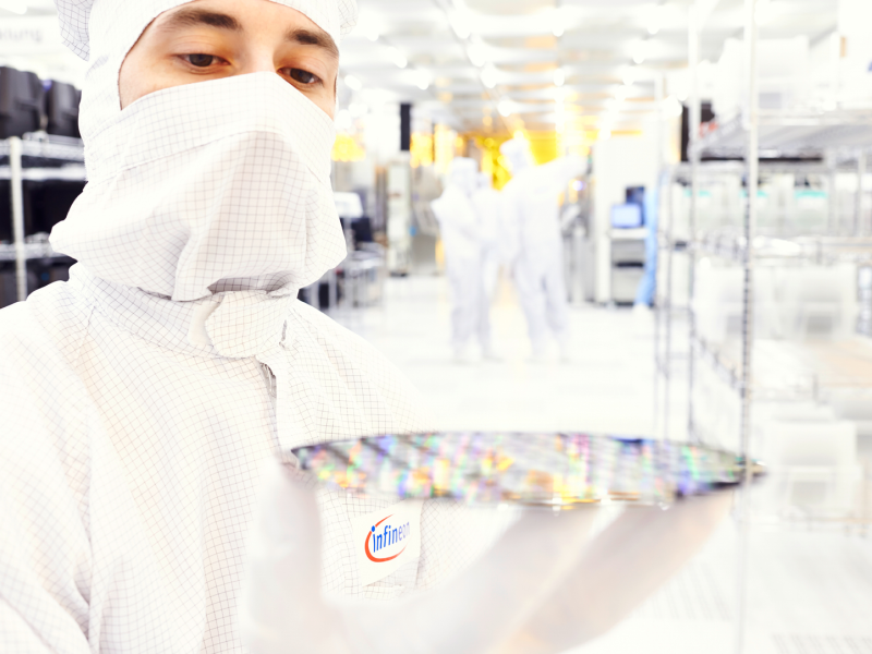
As part of the All2GaN Project, NanoWired aims at enhancing the efficiency of GaN HEMTs by utilizing Flip Chip technology. The performance evaluation of a synchronous buck converter clearly demonstrates the benefits of this approach: NanoWired Flip Chip GaN significantly reduces losses compared to traditional wire bonding. The half-bridge HEMT devices here are designed and developed by imec using their 100V GaN-IC technology platform.
At the same output current, the difference in efficiency is striking. At 2 A, the NanoWired Flip Chip GaN (400kHz) reaches 94% efficiency, while the wire-bonded version drops to 89%, meaning a 5% reduction in losses. At 4 A, the efficiency gap widens, with the NanoWired Flip Chip maintaining 91% efficiency, while the wire-bonded version falls below 85%, leading to over 6% lower losses. As current increases, the losses in the wire-bonded version rise significantly due to longer current paths and higher inductance, whereas the NanoWired Flip Chip maintains higher efficiency thanks to its optimized electrical design.
The assembly process involved growing NanoWires on the substrate and sintering the chip onto the substrate using KlettSintering, ensuring a highly reliable and low-resistance connection. The buck converter was built, and the characterization was carried out at Silicon Austria Labs (SAL), confirming these remarkable performance improvements.
By replacing traditional wire bonding with NanoWired Flip Chip technology, NanoWired enables next-generation power electronics with lower losses, higher efficiency, and superior thermal performance.
In the ALL2GaN project, Signify aims to reduce the size and or the power losses of its LED drivers by introducing Gallium Nitride (GaN) devices. Only the lower output capacitance of GaN devices can already help to reduce the circulating current in the resonant tank. This will result in lower losses and or size reduction. Further size reduction can be obtained by increasing the switching frequency. At Signify Research a 1000W LED driver prototype with a switching frequency up to 1 MHz has been designed, built and evaluated. Next to evaluating GaN devices at 1 MHz, this involved the design of magnetics for 1 MHz and EMC analysis. The picture below shows a GaN LED driver recently released in the market: a 320 W outdoor driver for the US market. Making use of the lower output capacitance of GaN devices combined with doubling the switching frequency, it was possible to increase the power level from 180 W to 320 W while reducing the housing size by 50%.
In the ALL2GaN (Affordable smart GaN IC solutions for greener applications) project, we aim to advance the performance of industrial Gallium Nitride (GaN) devices and system-on-chip technologies operating at 100 V or less. The main component in the fabricated IC’s is p-GaN gate High Electron Mobility Transistor (HEMT) power device. In Fig. 1(a) a X-sectional image of the p-GaN gate architecture of the device is depicted. With an optimization in the device fabrication imec Belgium has significantly reduced forward gate leakage, as shown in Fig. 1(b), comparing a transfer characteristic from the baseline device to the obtained improvement within ALL2GaN. The improvement in the gate characteristic, improves the gate robustness and reliability of the p-GaN gate HEMTs. Furthermore, Fig. 1(c) presents a good OFF-state gate and drain leakage of the fabricated devices. To showcase this technology further, power switches and integrated circuits (ICs) will be packaged and tested as part of the project.
(a) (b) (c)
Fig. 1. (a) X-section p-GaN gate used in imec’s 100 V power HEMT devices, (b) Transfer characteristics and (c) OFF-state drain and gate current of baseline and improved p-GaN gate HEMTs.
Heraeus Electronics is proud to announce that it will host an upcoming ALL2GaN event on April 9-10, 2024, at its facilities in Hanau. This event will focus on the groundbreaking developments in high-efficiency power electronics, particularly focusing on the capabilities of GaN chips to revolutionize the industry with higher efficiency, power density, and smaller sizes.
A nice open-access paper from the ALL2GaN consortium: Floating Capacitor Integrated DAB for Single-Phase, Single-Stage PFC in Wireless Battery Charging Application (Open Access)
To tackle the climate crisis, Infineon in Villach is launching two European research projects with enormous thrust: The "ALL2GaN" project is about easily integrated energy-saving chips made of gallium nitride.
We use cookies and similar technologies (also from third parties) to collect your device and browser information for a better understanding on how you use our online offerings. Details are available in our privacy policy where you can also change your preferences on cookies at any time.
These cookies are necessary for the website to function and cannot be switched off in our systems. They are usually only set in response to actions made by you, which amount to a request for services, such as setting your privacy preferences, logging in, or filling in forms.
Protects against cross-site request forgery attacks.
Retention period: This cookie only persists for the current browser session.
Saves the current PHP session.
Retention period: This cookie only persists for the current browser session.
The performance and effectiveness of content that you see or interact with can be measured.
The data collected is not used for any other purpose than analytics, visitors aren’t tracked across websites, fingerprints change daily for every visitor.