Attolight AG provides cathodoluminescence (CL) -based solutions for semiconductor in-line defect inspection and high-end material research in industrial R&D and academia.
Company profile
Attolight AG is an emerging leader in defect inspection for advanced semiconductor materials and devices using cathodoluminescence spectroscopy. The company designs and manufactures automated solutions for semiconductor in-line defect inspection and high-end material research tools for industrial R&D and academia. Attolight's core expertise lies in the application of quantitative cathodoluminescence (q-CL), a non-destructive characterization method that produces spectroscopic data at the nanoscale and provides a deeper understanding of the structure of materials.
The company's technology has a wide variety of applications in different areas such as reliability and performance analysis of LEDs, GaN power transistors, deep UV emitters, lasers, solar cells, and biosensors. The company has a global presence with systems in Europe, Asia, and North America, and is headquartered at the EPFL Innovation Park in Lausanne (Switzerland). Attolight AG offers a wide range of products from CL add-ons for TEM to a SEM-CL multi-spectroscopies platform and in-line solutions. On the SEM-CL platform, two analysis modes are proposed: continuous and time-resolved. The continuous mode is mainly used for the identification of the composition, dopants, defects... in materials while the time-resolved mode allows to study the dynamics of electronic recombination. This mode requires a time-resolved detector such as a streak camera.
The company designs and manufactures automated solutions for semiconductor in-line defect inspection and high-end material research tools for industrial R&D and academia.
Role in the project
Attolight is involved in two complementary tasks centered around the characterization of dislocations and other material defects:
- Exploration of analytical & intrinsic aspects of dislocations,
- Enable fab-based near-line analytical characterization during R&D, ramp-up & production.
Key contribution
ATT performs CL with two main goals in mind:
- Threading dislocations type and density in GaN-on-Si
- Point defects nature and clustering behavior characterization
Building on the threading dislocations results ATT will attempt to industrialize this application on its Säntis full wafer tool to enable large scale wafer inspection.
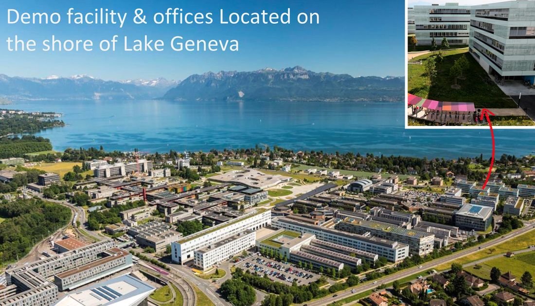
Attolight AG
EPFL Innovation Park, Building D
1015 Lausanne
Switzerland
attolight.com
Other Consortium Partners