Institut für Mikroelektronik Stuttgart (IMS) researches and developes innovative applications in micro-electronics and nano-technology. Being a member of the Innovation Alliance Baden-Württemberg, we engage in technological transfer to industry and combine university research and industrial applications by supporting reliable small-series production.
Company profile
Institut für Mikroelektronik is a foundation recognized as a non-profit organization under civil law with its headquarters on the Stuttgart-Vaihingen research campus. The research facility is a member of the Innovationsallianz Baden-Württemberg (innBW), a cooperation among twelve contract research organizations in Baden-Württemberg. The foundation’s mission is to conduct research and development in the field of microelectronic circuits and systems (silicon technology, customized circuits (ASIC), nano-structuring and image sensor technology) and to ensure that the results of its work are implemented in industrial practice. This task particularly includes:
- the construction and operation of research and development facilities for the design of microelectronic circuits and systems
- the construction and operation of process lines for the production of microelectronic experimental, sample and prototype circuits
- the execution of research and development projects on behalf of the federal government, the states and research institutions
- the promotion of practical training of scientific and technical personnel in the field of microelectronics
The foundation’s mission is to conduct research and development in the field of microelectronic circuits and systems and to ensure that the results of its work are implemented in industrial practice.
Role in the project
IMS is a collaborative partner mainly involved in WP1 and is focusing on stabilizing its GaN process on different substrates including alternative GaN-specific substrates. The focus of this work lies in the development of devices and circuits for 200V application. Due to its test capabilities, IMS will also have a supporting role in WP4 and WP5.
Key contribution
IMS will research and further develop the process-safe handling of alternative substrates, the structuring of GaN layers on alternative substrates and new innovative structures for the functionalization of GaN components. The so far very critical iterative development of processes and process parameters as well as the direct measurement and characterization of the results will be accelerated and optimized by so-called fast-loop processes. Due to its own know-how in assembly and interconnection technology and in test and reliability investigations on components, the IMS also contributes to the corresponding WP4 and WP5.
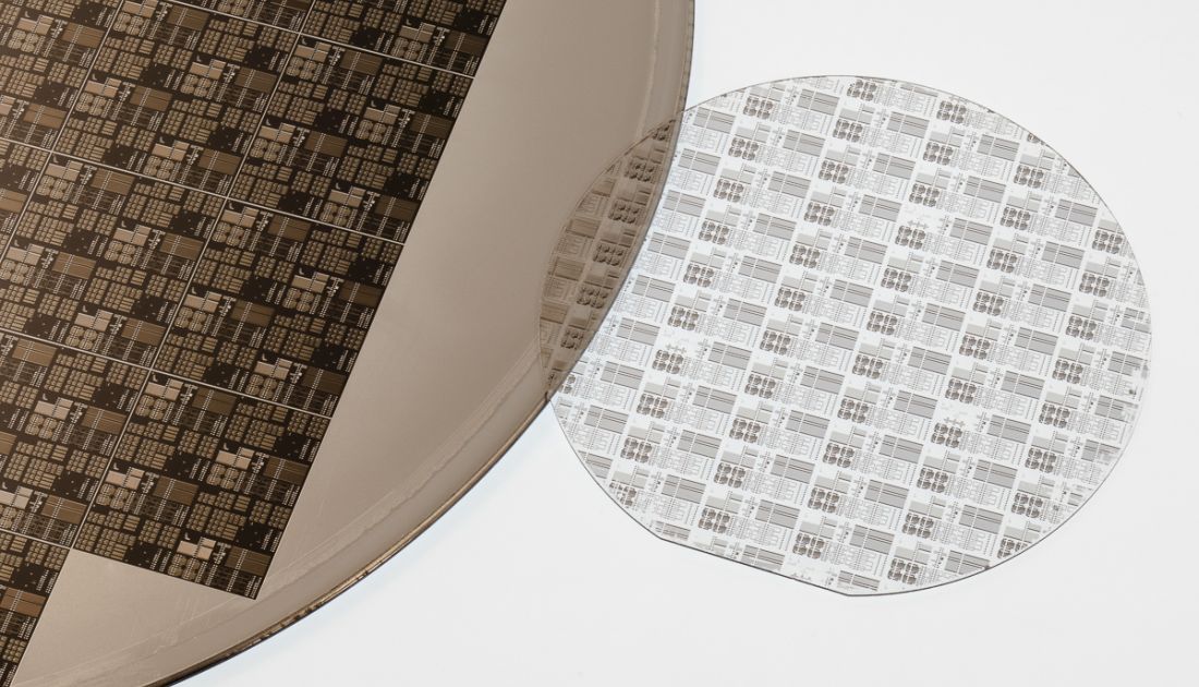
In coordination with the collaborative partners, the IMS conducts research on GaN substrates within WP1 based on different base materials: Silicon (Si), Silicon to Carbide (SiC) and on so-called Engineered Substrates (ES). These GaN substrates are functionally patterned by IMS using appropriate lithography processes. This includes mask-based lithography as well as direct-write processes. This work is performed with tools available at IMS. The processed substrates will be measured and characterized at IMS and the results discussed with the collaborative partners. The structuring of the GaN substrates to be processed by IMS is carried out on the one hand with special layouts specified by the collaborative partners, but also with established reference layouts and on the other hand with novel nanostructures, so-called "nanoholes", which IMS has developed and patented. With these structures, IMS expects a breakthrough in the functionalization of D-mode and E-mode devices on alternative substrates. Technologically, the realization of the nanoholes is very challenging and will be researched and developed on electron beam lithography.
IMS Chips
Allmandring 30a
70569 Stuttgart
Germany
www.ims-chips.com
Other Consortium Partners